Batch Wet Processing for Semiconductor Cleaning and Wet and Dry Etching
Batch wet processing is applied in semiconductor manufacturing and pilot environments for cleaning and wet etching steps where throughput and operational efficiency are primary drivers. By processing multiple wafers simultaneously, batch systems support stable, repeatable execution of well-defined process steps.
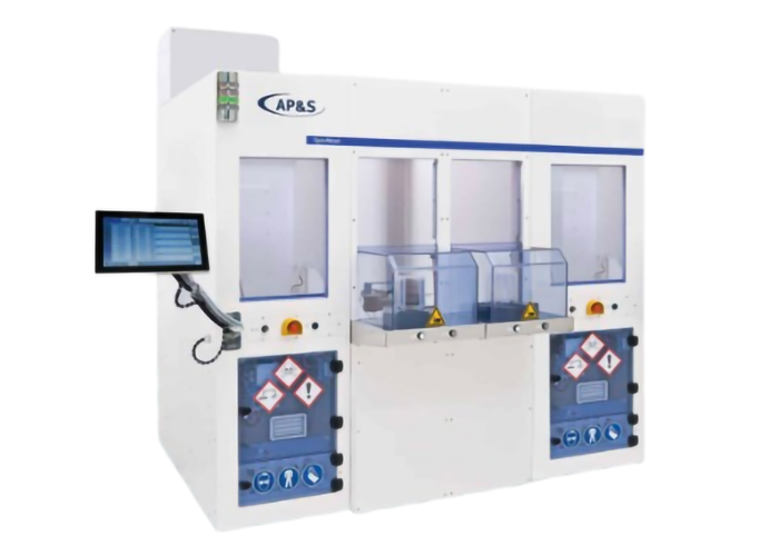
MDC Europe provides batch wet processing solutions configured for safe chemical handling, process consistency and integration into industrial and pilot workflows.
uniform treatment across multiple wafers is acceptable
throughput and cost efficiency are key priorities
individual wafer-level control is not required
This approach is common in established front-end and back-end process steps.
Typical Batch Wet Processing Applications
Wafer cleaning and surface preparation
Wet etching of silicon and dielectric materials
Photoresist residue removal
Front-end and back-end semiconductor processing
Different processing modules
High throughput wet processing
Up to 300 mm
Up to 100 wafer per run
Dry in Dry out
NID for IPA drying in combination with N2
Electroless metallization with nickel, palladium and gold
MDC Europe Expertise in Wet Processing
With experience across both batch and single wafer technologies, MDC Europe delivers wet processing solutions adapted to research, pilot and manufacturing environments. Our teams support system definition, configuration and long-term operation.
Why to Choose Our Products?
OEM-level refurbishment meeting original specifications
30+ years of experience in semiconductor solutions
Fast European delivery and support
Comprehensive product portfolio from spares to systems