Chucks and Wafer Holding Solutions for Semiconductor Manufacturing and R&D
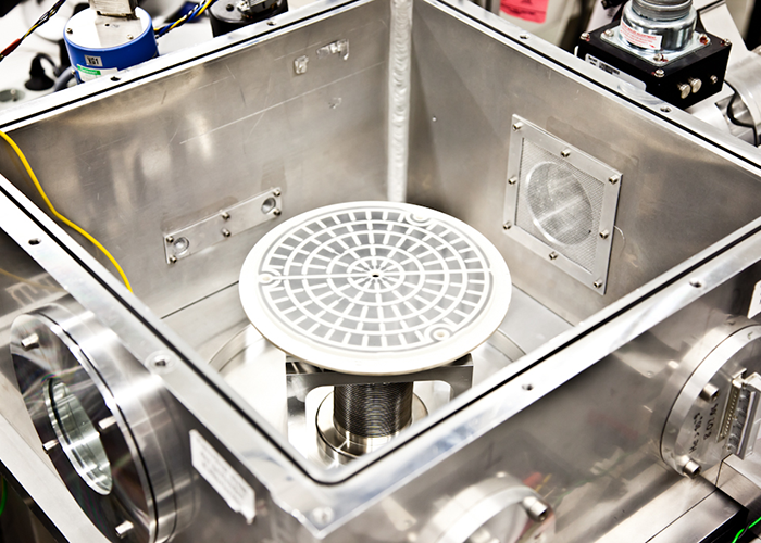
Wafer chucks are critical interfaces between the wafer and semiconductor process tools, directly impacting positioning accuracy, thermal behavior and process stability. They are deployed across lithography, deposition, etch and inspection platforms where mechanical and electrostatic performance must meet strict tool and process requirements.
MDC Europe provides wafer chuck solutions configured for specific semiconductor equipment platforms. Our portfolio supports tool integration, refurbishment and replacement strategies in production, pilot and advanced process development environments.
Process Role of Wafer Chucks
In semiconductor manufacturing workflows, wafer chucks are selected based on:
tool platform compatibility
positioning accuracy and flatness requirements
electrostatic and thermal behavior under process conditions
Chuck performance directly affects overlay accuracy, process repeatability and tool uptime.
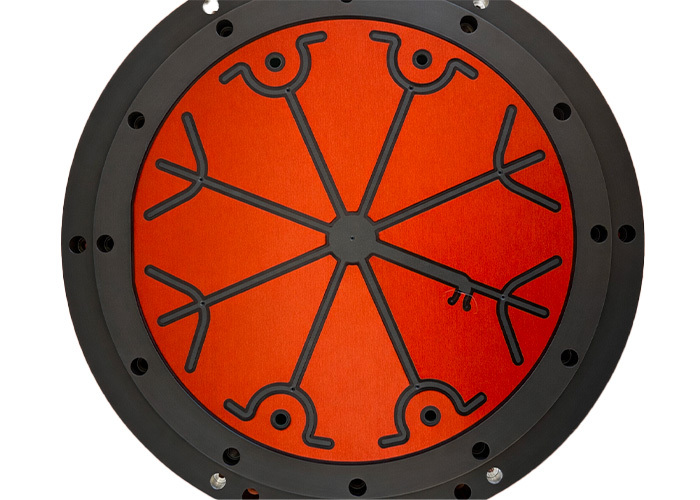
Chuck Solutions by Tool Platform
MDC Europe supports wafer chuck solutions aligned with specific semiconductor equipment environments including:
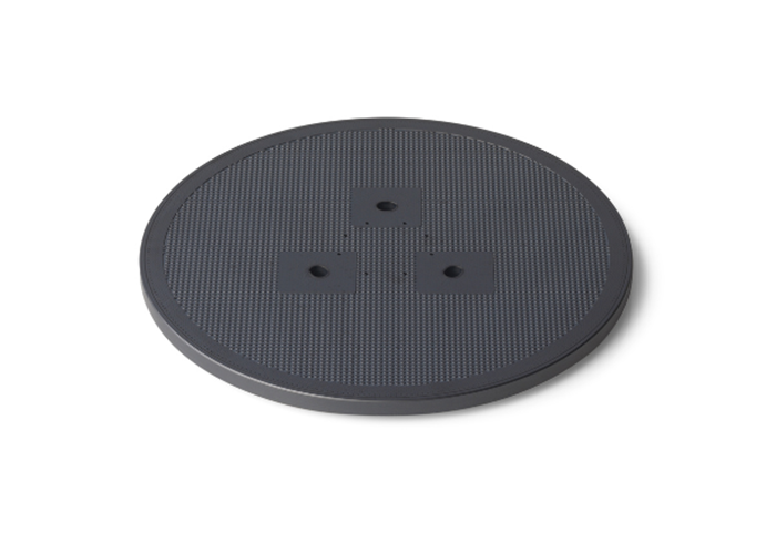
ASML Exposure Chuck
ASML exposure chuck for wafer positioning and stability in lithography exposure tools.
MDC Europe supports chuck selection, refurbishment and integration based on tool specifications and process constraints, ensuring compatibility and stable operation in semiconductor manufacturing environments.
Why to Choose Our Products?
OEM-level refurbishment meeting original specifications
30+ years of experience in semiconductor solutions
Fast European delivery and support
Comprehensive product portfolio from spares to systems